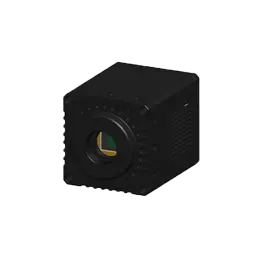
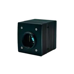
The characteristic of CCD image sensor is to fully keep the signal without distortion during transmission (exclusive channel design). By collecting each pixel to a single amplifier and then performing unified processing, the integrity of the data can be maintained; CMOS image sensor has no exclusive channel design, so we must zoom in first and then integrate the data of each pixel. On the whole, the difference in the applications of CCD and CMOS image sensor designs is reflected in the imaging effect, and the differences are specifically manifested in the following aspects.
Since each pixel of sensor CMOS includes an amplifier and A/D conversion circuit, too many additional devices compress the surface area of the photosensitive area of a single pixel. Therefore, under the same pixel, the sensitivity of CMOS will be lower than that of CCD with the same size of the photoreceptor.
Since each photosensitive diode of sensor CMOS is equipped with an ADC amplifier, if it is counted in megapixels, more than one million ADC amplifiers are needed. Although it is a uniformly manufactured product, each amplifier is more or less slightly different, it is difficult to achieve the effect of in-step amplification. Compared with a CCD with a single amplifier, sensor CMOS finally calculates more noisy point.
The structure of each pixel of sensor CMOS is more complicated than that of CCD, and its photosensitive aperture is not as large as that of CCD. When comparing CCD and CMOS photoreceptors of the same size, the resolution of CCD photoreceptor is usually better than that of CMOS. However, the current CMOS photosensitive originals in the industry can achieve the design of 14 million pixels/full-frame, and the quantitative advantages of CMOS technology can overcome the difficulties in manufacturing large-size photosensitive originals.
CMOS applications can integrate all peripheral facilities in a single chip at one time, saving the cost of processing the chip and the loss of pass rate; compared to CCD which uses the method of charge transfer to output signals, another transmission channel must be established. If there is a failed pixel in the channel, it will cause the signal to be unable to be transmitted, so the pass rate of CCD is lower than that of sensor CMOS. Coupled with the exclusive transmission channel design, the manufacturing cost of CCD is relatively higher than that of sensor CMOS.
The image charge driving method adopted by sensor CMOS is active, and the charge generated by the photosensitive diode is directly amplified and output by the transistor beside it; but the CCD adopts the passive method, and a voltage must be applied to allow the charge in each pixel to move to the transmission channel. The applied voltage usually needs to be above 12 volts (V). Therefore, the CCD must have a more precise design of power supply circuit and high withstand voltage strength. The high driving voltage makes the CCD's power much higher than that of sensor CMOS.


