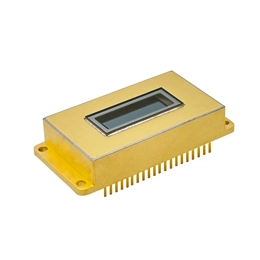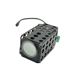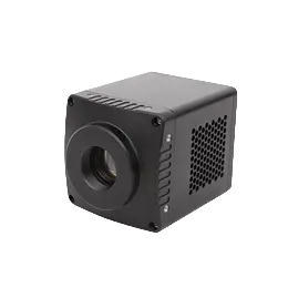
In today's increasingly advanced technological landscape, the demand for high-quality semiconductor chips continues to grow. As a crucial component in various industries, including electronics, automotive, healthcare, and aerospace, ensuring the highest level of accuracy and reliability in semiconductor inspection is of paramount importance. One technology that has emerged as a game-changer in this area is the CMOS Linear Image Sensor.
Semiconductor inspection plays a vital role in maintaining the quality and functionality of chips used in different applications. Any defects or anomalies in the manufacturing process can lead to costly failures, impacting both manufacturers and end-users. To overcome these challenges, the integration of CMOS Linear Image Sensors has revolutionized the way infrared semiconductor inspection is performed.
CMOS Linear Image Sensors offer several advantages over traditional imaging solutions, making them highly sought-after in the semiconductor inspection industry. One notable benefit is their high resolution, enabling the detection of even the tiniest defects with exceptional accuracy. These sensors also provide improved sensitivity and dynamic range, allowing for precise identification of defects across varying semiconductor materials and conditions.
Another advantage of CMOS Linear Image Sensors is their ability to capture images at high speeds, ensuring rapid inspection and increased production throughput. Additionally, these sensors offer better noise performance, reducing false rejects and minimizing errors in defect inspection. These combined features make CMOS Linear Image Sensors an ideal choice for semiconductor manufacturers looking to enhance their inspection accuracy.
The applications of CMOS Linear Image Sensor in semiconductor inspection is vast. These sensors are integrated into advanced inspection systems, enabling real-time and non-destructive monitoring of semiconductor wafers. By capturing high-resolution images of the wafers, CMOS Linear Image Sensors facilitate thorough analysis and quick identification of potential defects, such as cracks, scratches, or contamination.
Moreover, CMOS Linear Image Sensors excel in inspecting the uniformity of critical features on the wafers, ensuring that the etching or deposition processes have been executed accurately. By detecting abnormalities at early stages, manufacturers can take immediate action to rectify any issues and prevent costly production stoppages or defective products from reaching the market.
The semiconductor industry heavily relies on accurate and reliable inspection processes to ensure optimal chip performance. CMOS Linear Image Sensors have emerged as a key technology in this domain, offering numerous advantages over traditional imaging solutions. With their high resolution, sensitivity, speed, and noise performance, these sensors enhance ir semiconductor inspection accuracy, enabling manufacturers to detect defects in real-time and optimize their production processes. As the demand for high-quality semiconductor chips continues to rise, CMOS Linear Image Sensors play a critical role in meeting industry demands and delivering superior products to end-users.


